![]()
 The Semiconductor Physics research group (“SemPhys”) is part of the Department of Physics at the University of Strathclyde. The Department is a member of the Scottish Universities Physics Alliance (SUPA).
Research sub-groups
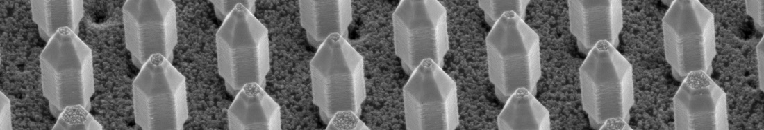
Semiconductor Quantum Electronics (SEQUEL)
- Semiconductor nanoscale systems
- Quantum computing and quantum electrical metrology
- Electrical initialisation and readout of spin qubits in SiC
- Empowering Practical Interfacing of Quantum Computing (EPIQC)
- See sequel.phys.strath.ac.uk
Advanced Materials Diffraction (AMD) lab
![]()
- Advanced electron diffraction of semiconductors and crystalline materials
- Techniques include electron backscatter diffraction and electron channelling contrast imaging
- Characterisation of crystal defects and crystal properties (structure, elastic strain, (mis)orientation, crystal polarity)
- See amd.phys.strath.ac.uk
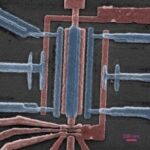
Gallium Oxide Optoelectronic Devices (GOOD)
![]()
- Wide bandgap semiconductor and defect characterisation
- Ultraviolet (UV) detection technologies
- Low-cost production of UV sensing materials
- See good.phys.strath.ac.uk
Experimental Quantum Nanoscience Lab (EQNL)
- Physics and applications of polariton condensates in microcavities
- Solid-state quantum systems for quantum information and nanophotonics
- Hybrid polariton-quantum dot platforms for scalable quantum hardware
- See eqnl.phys.strath.ac.uk
Microscopy & Spectroscopy of Semiconductors
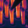
- Characterisation of UV-vis LEDs & microLEDs, transistors, solar cells, nanostructures, etc.
- Specialised capabilities in cathodoluminescence (CL), X-ray microanalysis (WDX/EDX), electron beam induced current (EBIC) and nanoprobing
- Innovative combinations of techniques to study the same micron-scale area
- See the Physics Electron Microscope Facility page
🥼 Join us! Jobs / PhD studentships available
- Funded PhD studentships are often available. See the different sub-groups for current vacancies.
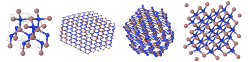
💎 Interactive crystal models
Explore crystal structures, lattice planes and dislocations
🧮 Crystallographic calculator
Convert between Miller and Miller-Bravais plane and direction indices, calculate angles between lattice planes, and obtain normal directions of planes in for cubic and hexagonal lattices. See here.
📖 Latest publications
-
![[doi]](https://semphys.phys.strath.ac.uk/wp-content/plugins/papercite/img/external.png) Imaging misorientation and strain of single dislocations in GaN using electron backscatter diffraction
Imaging misorientation and strain of single dislocations in GaN using electron backscatter diffraction - Controlling point defect populations in AlGaN deep UV LEDs
- Microanalysis of $\beta$-(AlₓGa₁₋ₓ)₂O₃ films grown by MOCVD
- Trion quantum coherence in site-controlled pyramidal InGaAs quantum dots
- Gallium oxide-based photodetectors for water quality monitoring
- Reproducibility and variability in commercial SiC MOSFETs at deep-cryogenic temperatures
- Molecular beam epitaxy of boron arsenide layers
- Strain-induced modifications of thin film silicon membranes by physical bending
📰 Group news
- October 2025: Well done to Stefan Nicholson, who has successfully defended his PhD thesis. His work on perovskite solar cells was undertaken jointly between SSD and the group of Dr Aruna Ivaturi in the Department of Pure and Applied Chemistry.
- March 2025: Congratulations to Dr Fabien Massabuau who has won the Materials Young Investigator Award.
- October 2024: Welcome to Farnaz Hadizadeh who joins the GOOD group as a PhD student with Diamond Jubilee Research Scholarship.
- August 2024: Welcome to Mohammed Alessa who joins the GOOD group as a PhD student.
- June 2024: Welcome to Adam McMorris who won a Carnegie Vacation Scholarship for conducting a summer project in the GOOD group.
- April 2024: Welcome to Sean Douglas who joins the group as a post-doc working on project “Tuneable radiation-resilient (AlGa)2O3 UVC photodetectors” funded by the UK Space Agency.
- Older news items are archived here.